3# Board Commissioning Instructions
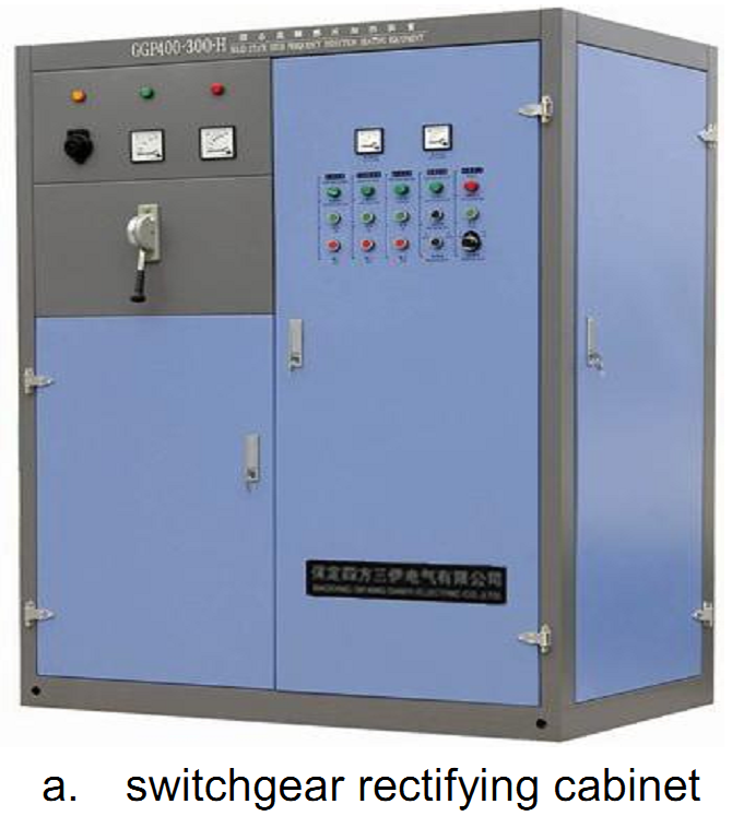
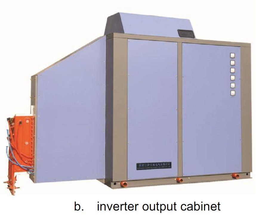
GGP series of solid state HF welder compositon
A: Check The Wiring Between Boards
① Check the rectifier board,Whether the terminal wiring of board 3#, board 9# and board 2# is correct.
Check whether the inverter pulse output line of board 3 # is connected in order
The order is:
From left to rightX4~X7 Sequential connection311、312、314、313;
Two of the four trigger pulses of board 3# are the same, and the connection sequence must not be mistaken! Otherwise, short circuit tripping fault occursduring startup.
② Terminal connection
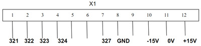
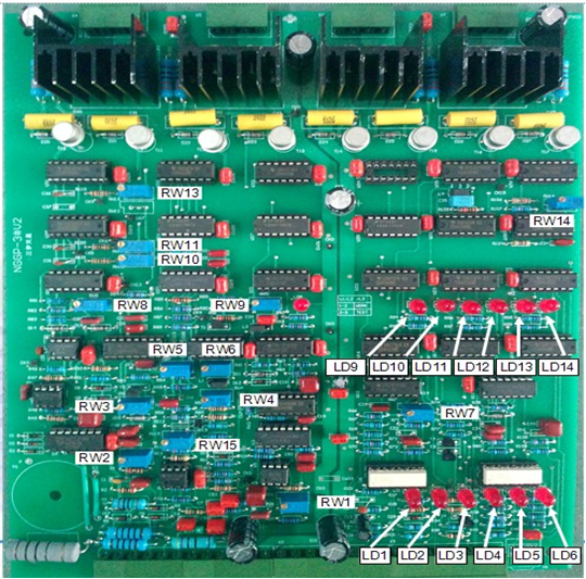
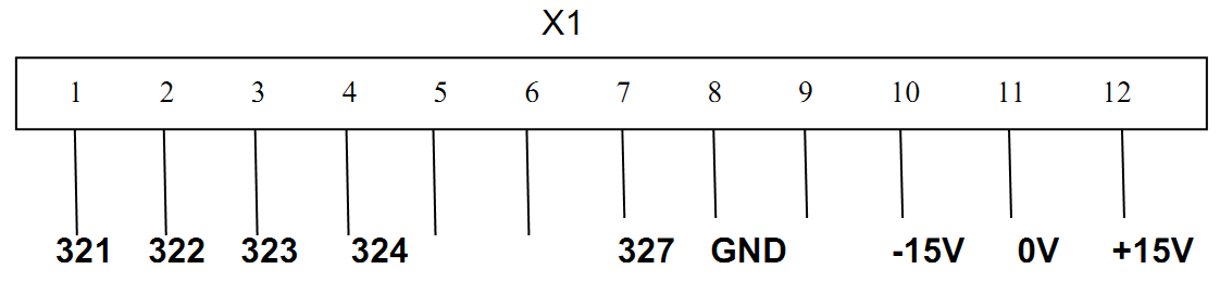
X1The Terminals Connection Sequence:
(321,322)- The phase-locked signal from the slot circuit comes, from the phase-locked magnetic loop;
(323,324) - Open protection signal, AC output sampling magnetic ring from inverter output(Or connect 1 channel of AC protection signal on the 9# board tothis,Increase the parallel resistance);
(327,GND) - Protection seal pulse signal from 9# board;
③ X2 terminal with new 3#borad are the same;The 1st and 2nd bits of X3 terminal are empty,Bits 3 and 4 are connected to 919 and 900,Bits 5 and 6, 7 and 8 are connected to 24V and GND
B: Check The Control Power Supply Is Normal Or Not
Send the control power supply, and use a multimeter to measure the voltage of + 15V, - 15V to 0V of the new 3 board,Allowable range:15.3~15.5V。
C: Check Pulse Consistency
Simultaneously measure the odd layers from top to bottom on the front bridge side with an oscilloscope,,And the driving waveform of even layer MOS transistor from top to bottom on the negative Bridge side.The front and rear edge error is less than±10ns.
Use an oscilloscope to simultaneously measure the even number of layers and from top to bottom on the front bridge side,Driving waveform of odd layer MOS transistor from top to bottom on negative Bridge side.The front and rear edge error is less than±10ns.
Note: pulse consistency is very important. During measurement, the scale of oscilloscope must be below 50ns for accurate measurement
D:Dead Band Setting
Measure the driving waveforms of odd and even layer MOS transistors on the positive or negative Bridge side at the same time with an oscilloscope probe, And adjust RW10 so that the dead time is not less than 220ns.
E:Phase Locked Voltage Setting
Adjust RW3 so that the phase-locked voltage of CK3 to CK0 is9.6~9.7V。
F:Separate excitation frequency sweep determine the resonant frequency
Short circuit pins 1 and 2 of 3# board pins L2, L3 and L4,Short circuit of pins 2 and 3 of L1,Power and water transmission, and turn the DC voltage to 50V,Adjust RW4 other excitation sweep frequency and observe the size of DC ammeter,When the DC current is maximum, stop adjusting rw4, and the inverter frequency at this time is the resonant frequency f0.
G:Set Upper And Lower Limits Of Frequency
Short circuit pins 2 and 3 of 3# board pin L1,Adjust RW4 clockwise to the maximum, observe the upper limit frequency value, and adjust RW6 so that the upper limit frequency is 70 ~ 90khz higher than the resonance frequency.If not, the resistance value of R54 can be reduced. The smaller the resistance, the higher the frequency.
Adjust RW4 counterclockwise to the minimum and observe the lower limit frequency value,Adjust RW5 so that the lower limit frequency is 80 ~ 100kHz lower than the resonance frequency.If not, the resistance value of R53 can be increased.
The greater the resistance, the lower the frequency.Or change the C15 capacitance value. The larger the capacitance, the lower the frequency, but the upper limit frequency also decreases (not recommended)
H:Overclocking Protection Regulation
Short circuit pins 2 and 3 of 3# board pins L1 and L3,Adjust RW4 clockwise to make the output frequency reach the upper limit frequency,Adjust RW1 so that the voltage between CK1 and CK0 is 10V,Adjust RW7 so that the voltage from CK14 to CK0 is 9.8v
I:Phase Lock, Inverter, Angle Adjustment
① Short circuit pins 1 and 2 of 3# boards L1, L2, L3 and L4, self excitation
② Start heating to DC voltage 60V and observe whether the inverter voltage waveform vibrates.If the display frequency is close to the resonance frequency excited by it, it indicates that the vibration has been started,At this time, the resonant frequency and inverter waveform of rw13 will change significantly.
If the inverter frequency is at the upper limit and there is no change in the waveform of RW13, stop the heating, exchange the positions 321 and 322, and then start the heating to observe whether it is phase locked.
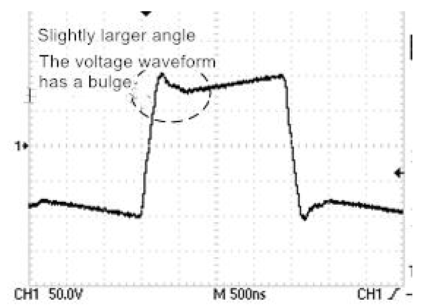
③ After starting the vibration, turn the DC voltage to 100V, observe the output waveform of the inverter voltage as shown in the figure below, adjust RW13 to make the inverter waveform as shown in figure (c), and store it with an oscilloscope.
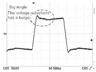
(a)The perceptual angle is very large

(b)The perceptual angle is very large
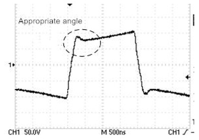
(c) Appropriate angle
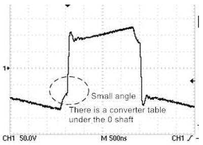
(d)Small angle
Stop heating, the potentiometer does not move, repeat starting and stopping for 5 times, and observe whether the vibration starts normally
J:Open Protection Commissioning
① Short circuit pins 1 and 2 of 3# boards L1, L2, L3 and L4 ,self excitation.
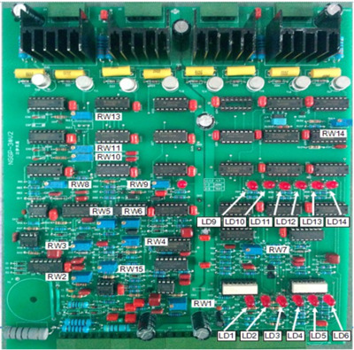
② Start heating to DC voltage of 100 ~ 150V. At this time, adjust RW15 clockwise (on protection) to make LD2, LD4, LD5 and LD6 light up stably.
K.High And Low Out Of Lock Commissioning
①Adjust RW9 so that the low out of lock voltage of CK12 to CK0 is 9.3 ~ 9.6V.
② Adjust RW8 so that the high out of lock voltage of CK13 to CK0 is 10.3 ~10.5V。
③ After normal vibration, measure the voltage of CK4 to CK0, based on this, add 1.0V ~ 1.3V as the high out of lock protection value, and reduce 1.0V ~ 1.3V as the low out of lock protection value.
L.Overvoltage Protection Commissioning
After normal vibration, turn the DC voltage to 200V, adjust RW2 clockwise to protect the 3# board, measure the voltage of CK2 to CK0, and adjust RW2 counterclockwise to increase CK2 to CK0 by 2.5 to 3 times.
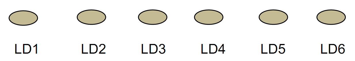
M.Work indicating lamp:
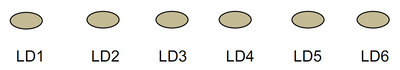
LD1:Reset indicator light, when the light is on, it means resetLD2:Self-excited indicator, the light is on and self-excited.
LD3:spare
LD4:3 # board normal indicator: when the indicator is on, it is normal; when the indicator is off, it is faulty;
LD5:Turn on the protection indicator light. When the light is on, the protection is on, and when the light is off, the protection is off.
LD6:Turn on the protection indicator light. When the light is on, the protection is on, and when the light is off, the protection is off.
N. Protection Indicator
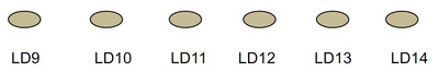
When the light is on, it is protection, and when the light is off, it is normal
LD9: Low Loss Of Lock
LD10:High Loss Of Lock
LD11:Overclocking Protection
LD12:Standby
LD13:Overvoltage Protection
LD14:Power Protection
Download - 3# ENG.pdf
3# RUS.pdf |